ELEC3020 - Lecture 2
Combinatorial & Sequential Circuits - Slides
Combinatorial vs Sequential
- Combinatorial -> no memory
- Equivalent to mathematical function
- Sequential -> feedback + memory
- Equivalent to computer program
De Morgan’s Theorem
- The complement of the logical AND of two or more variables is equal to the logical OR of the complements of those variables
- The complement of the logical OR of two or more variables is equal to the logical AND of the complements of those variables
(x + y)' = x'y'$$$$(x\ y)' = x' + y'
- Complement ?
Answer:Boolean algebra allows us to simplify a function so that it contains the smallest number of literals
Link to original
Combinatorial Circuits
- Arbitrarily complex circuits that can be built from basic gates
- Output only depends on the input lines
- No memory
Decoder
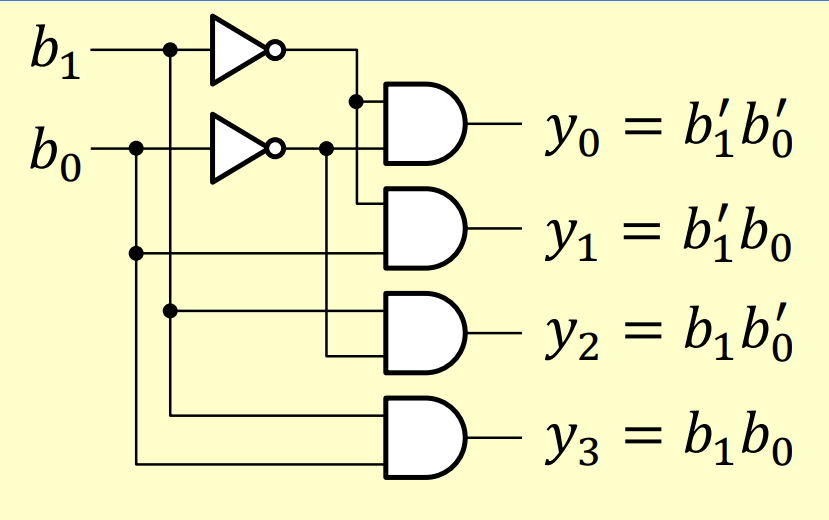
- A decoder is a combinational circuit that decodes input code and activates a corresponding output line
- Takes in inputs
- Has outputs
- Each input activates a single output
Each output is a minterm:
- Implementing decoder only requires AND gates + inverters
Implementing Boolean Functions with Decoders
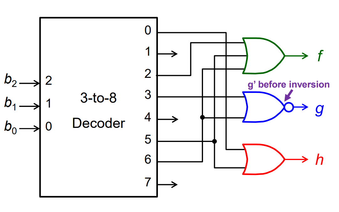
- Any Boolean function of input variables can be implemented using a -to- decoder and a logic gate
- Decoders can generate all minterms
- Decoder is particularly advantageous when multiple Boolean functions of the same input variables need to be implemented
Avoid large fan-in output gates:
- When there are fewer 1’s, use OR gate to implement function
- OR output lines for which function is equal to 1
- When there are fewer 0’s, use NOR gate to implement function
- NOR output lines for which function is equal to 0
Enable Input
Link to original
- Enable input controls the operation of the decoder
- If is not active, then all outputs have zeroes
- Ignores the inputs
- To add enable input to a decoder circuit, you just AND just before the output
Encoders
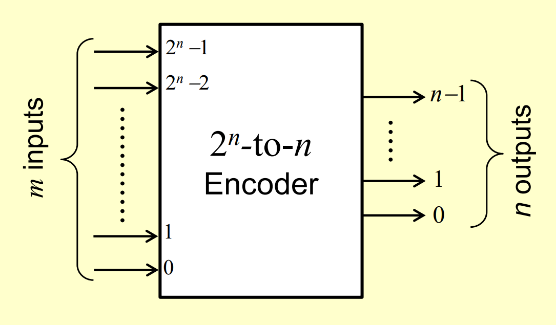
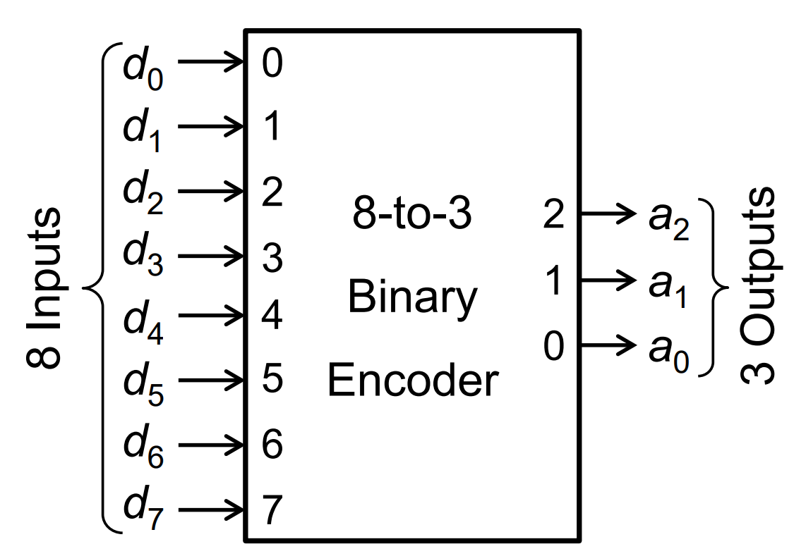
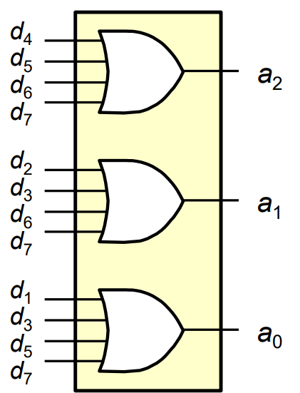
- Encoders are combinational circuits that perform opposite function of a decoder
- Generates an output binary code for the active input
- For correct operation, requires that only a single input line is asserted at any one time
- Simple encoders can be made with just OR gates:
Limitations
Link to original
- We assume only a single input line can be active at any time
- Having more than one input can create undesired outputs
- If no inputs are active, then the output is 000… which should usually only occur for when
Multiplexers
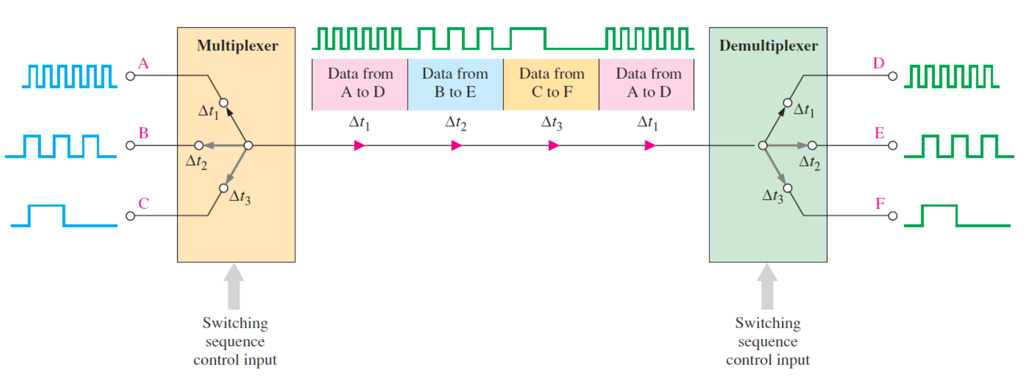
- Multiplexing and demultiplexing are used when data from several sources are to be transmitted over a single communication channel or medium and redistributed to several destinations
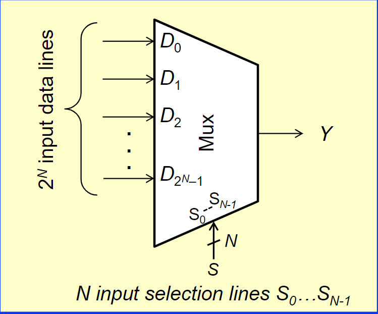
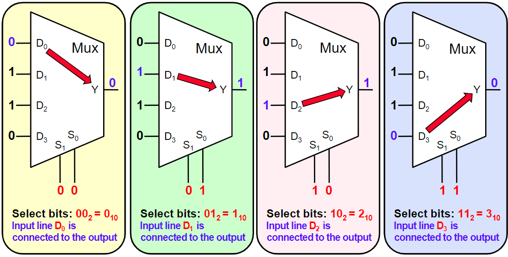
- A multiplexer is a digital circuit that selects and combines multiple input signals into a single output signal
- Also known as a data selector
Link to original
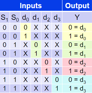
4-to-1 Multiplexer:
Note: there is an additional input/s that control which of the other inputs is connected to the outputTruth Table:
Demultiplexers
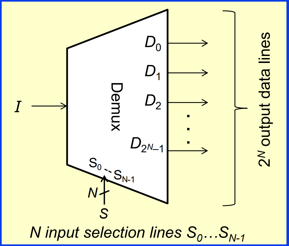
- A demultiplexer is a digital circuit that performs the opposite function of a multiplexer
- Takes single input, routes to one of several output lines
- Enable distribution of a single input to multiple destinations
Link to original
Half Adder
Link to original
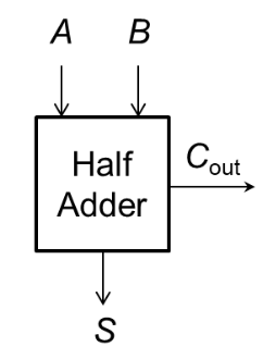
- Adds 2 input bits
- Outputs 2 bits:
- Carry bit
- Sum bit
Full Adder
Link to original
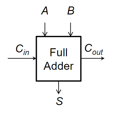
- Adds 3 bits
- Sum bit is 1 if the # of 1’s in the input is odd
- Carry bit is 1 if there are two-three “1” inputs
Tri-State
When a Tri-State is open, the output is ‘not connected’, represented with an asterisk. This is not an arbitrary output, but instead is a third output, distinct from ‘0’ and ‘1’ that indicates the switch is not enabled.
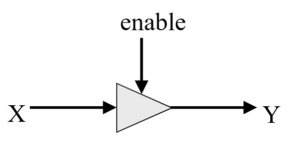
Otherwise, if enable is 1, the output equals the input . This is useful because sometimes we want to definitively know whether our switch is enabled or not instead of just receiving a ‘0’ output when off.
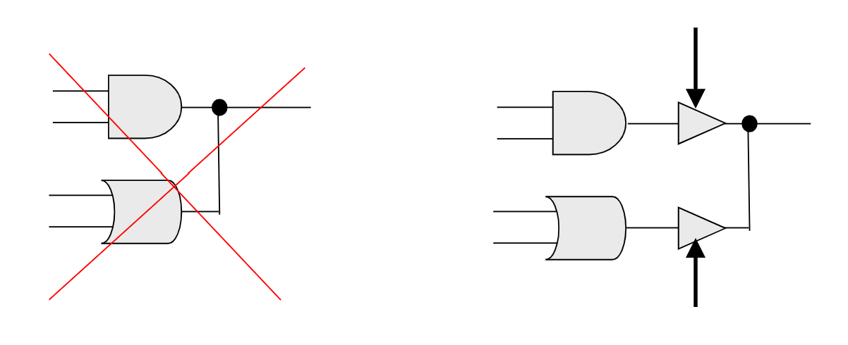
By setting output to “high ohm” when the circuit is OFF, we can prevent it from creating a short circuit if its connected to the same communication wire as another output. This is really useful as it allows multiple devices to share the same physical communication wire, known as a bus, without damaging each other or corrupting data.
High Ohm State
The “high ohm” state, also known as high impedance, effectively replicates the environment in which the wire has physically been “snipped” out of the circuit.
If multiple outputs are connected to the same wire, when they are in the high impedance state, then they do not impact the state of the wire. Any output can switch the entire wire to either a ‘0’ or ‘1’ state without causing a short circuit.This “high ohm” state can be considered a third alternate state distinct from ‘0’ and ‘1’. It cannot be treated as a ‘don’t care’ state.
Latches, Flip-Flops, Memory
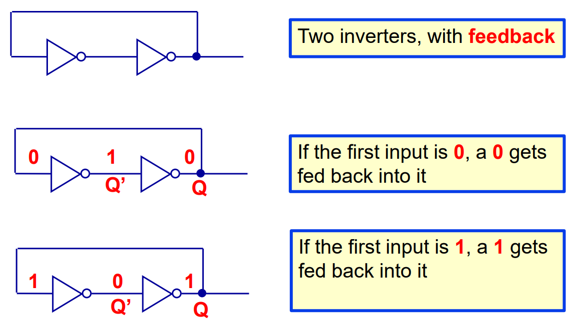
By implementing a feedback loop in a circuit, we can ‘trap’ a single bit of information. The circuit’s output now depends on the previous ‘state’ it was in. This is an example of the smallest instance of a memory cell.
A circuit with a feedback loop is called a sequential circuit.
Memory
Memory
Link to original
- Three properties to be considered memory:
- Holds values
- Able to read saved values
- Able to change saved values
- One-bit memory holds a single bit, 0 or 1
Storage
- Using loops, circuit outputs become inputs
Link to original
- Still extra steps needed to be considered memory
- We cannot change the value in the loop!
Latches
RS Latch
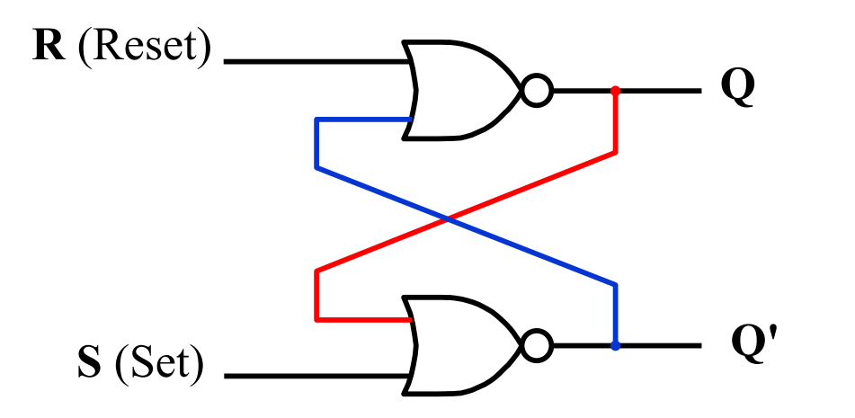
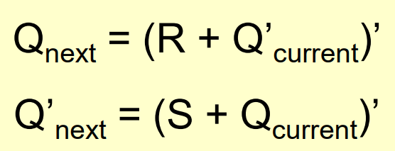
- Using NOR gates instead of inverters allows us to make a RS latch
- RS → Reset-Set
- The two inputs R and S let us control outputs Q and Q’
- Q and Q’ feed back into the circuit
Set Operation: RS = 01
- S → 1 → 0 → 1
i.e. set Q to 1- Outputs then stop changing
- Circuit becomes stable
Reset Operation: RS = 10
- R → 1 → 0 → 1
i.e. reset Q to 0- Outputs then stop changing
- Circuit becomes stable
Remember, there is propagation delay for all these changes
- R=S=1 should never be used
RS Latches are Memory
Link to original
- RS latch meets all of our criteria above to be considered memory
- The output Q is considered the state of the latch
- Represents the data stores
Enable (Gated) RS Latch
- Additional Enable input signal C is used:
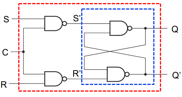
- Dotted blue area is the RS latch from last lecture
- Control input acts like an enable
- When C=0, latch remains in same state
- When C=1, normal latch operation occurs
An enabled latch is a level sensitive memory output may change a number of times depending on the duration of the enable pulse
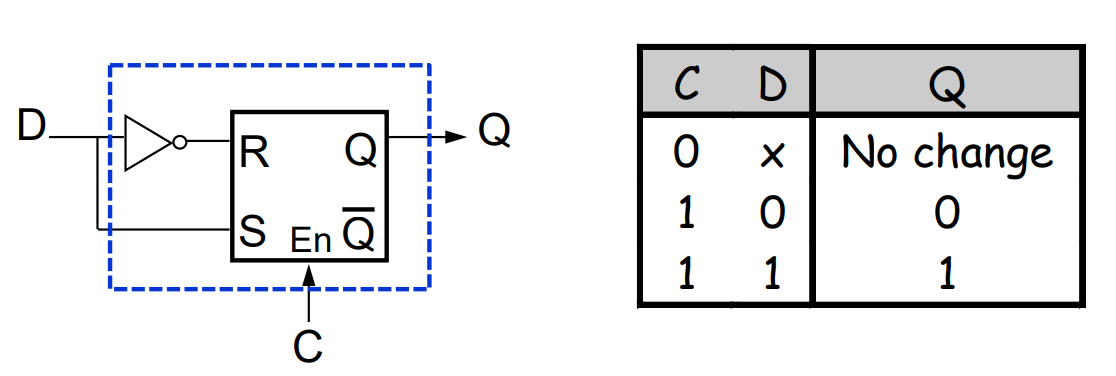
Enabled (Gated) D-Latch
- One data input
- S=D and R=D’
S RLink to original
Flip-Flops
Clocks and Flip-Flops
- For proper operation, latches must form flip-flops
- They can change state only at well defined times
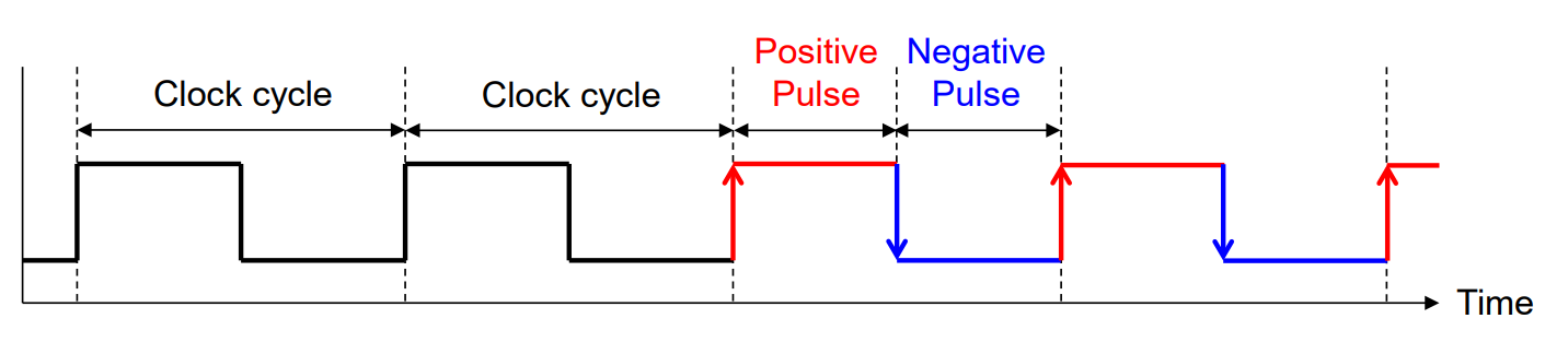
- Clocks are often used to synchronise circuits
- They generate repeating, predictable pattern of 0s and 1s
- If several circuits share a common clock signal, they can coordinate their actions with respect to one another
Link to original
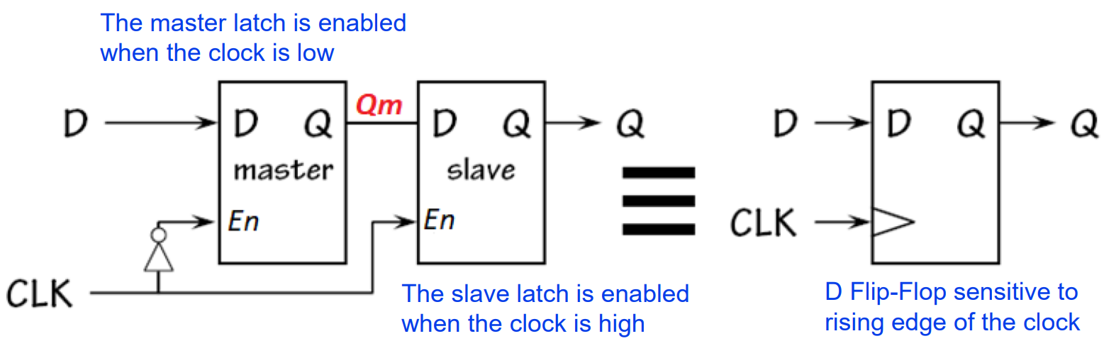
Master Slave D Flip-Flop
- Structure two D-latches connected in series
- The master latch is connected to the input D
- The slave latch is connected to output Q
- Controlled by inverted signal controlling master latch
- One latch is enabled at any given time
- The final output changes during one transition of clock
Edge-Triggering
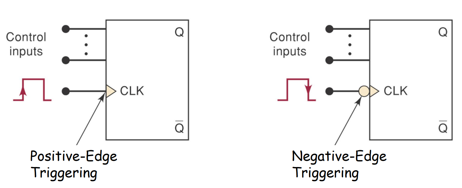
- Edge-triggering means the output change can happen only during clock pulse transition
- Noted using a triangle symbol
Link to original
- Two types: (see slides for diagrams)
- Positive edge-triggering output looks at input at the instant the clock transitions from low to high
- Negative edge-triggering output looks at input at the instant the clock transitions from high to low
Flip-flop Variations
Link to original
- There are many different flip-flops based on the D flip-flop
- Flip-flop examples:
- JK flip-flop inputs are used to complement current state
i.e. JK = 1 → current content is flipped
- Otherwise works as RS latch
- T flip-flop only maintain or complement its current state
i.e. T = 1 → current content is flipped
- Otherwise no change
- Characteristic tables on slides
Registers
Several Flip-Flops can be combined into one register. An -bit register is a group of binary storage cells (flip-flops).
Registers are classified according to the number of bits of storage and operating mode. The standard register type, which we will also be using, is parallel in parallel out (PIPO).
Registers are commonly used as temporary storage in a processor:
- They are faster and more convenient than main memory
- More registers can speed up complex calculations
Basic Implementation
Basic registers are easy to build:
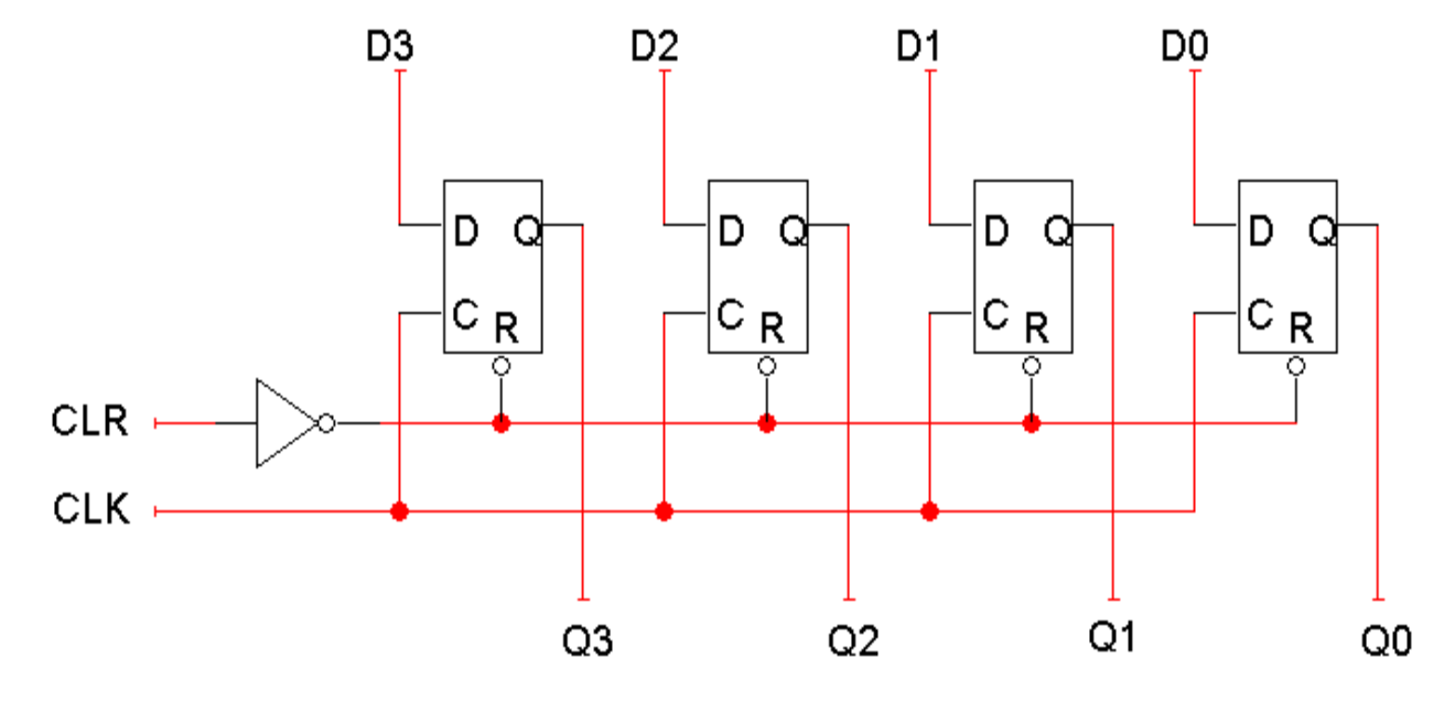
All flip-flops share a common CLK (clock) and CLR (clear) signal.
Shift Registers
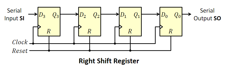
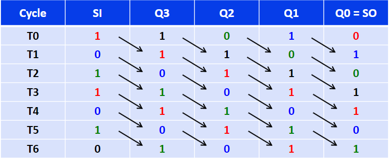
A shift register ‘shifts’ its output once every clock cycle. is an input that supplies a new bit to shift ‘into’ the register.
Shift Registers
- A shift register is a cascade of flip-flops sharing the same clock
- Allows data to be shifted from each flip-flop to its neighbour
- All bits are shifted simultaneously at the active edge of the clock
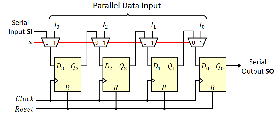
Parallel-In Serial-Out Shift Register
- Two control functions:
- s = 0 → shift (works like above)
- s = 1 → load data (update D for each flip-flop)
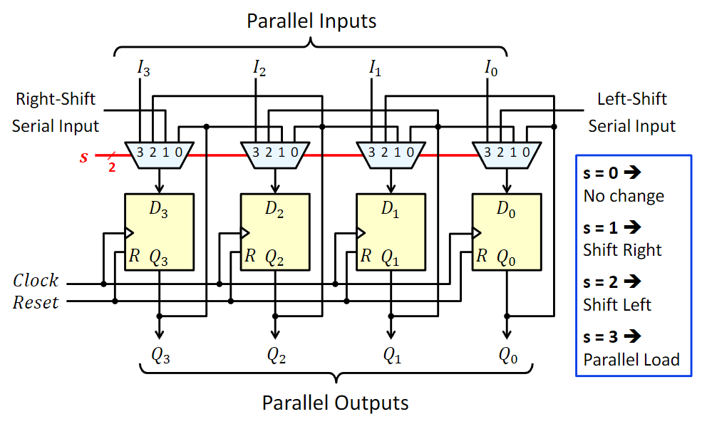
Universal Shift Register
- Four control functions:
- s = 00 → no change in value
- s = 01 → shift right (right-shift serial input)
- s = 10 → shift left (left-shift serial input)
- s = 11 → parallel load 𝑛𝑛 input bits
Link to original
Clock
Clocks and Flip-Flops
- For proper operation, latches must form flip-flops
- They can change state only at well defined times
- Clocks are often used to synchronise circuits
- They generate repeating, predictable pattern of 0s and 1s
- If several circuits share a common clock signal, they can coordinate their actions with respect to one another
Link to original
The Clock
Link to original
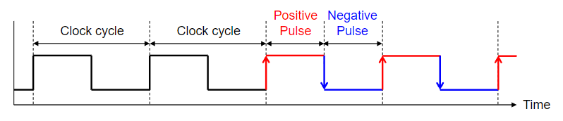
- Clock cycle (or period) is a time duration
- Clock frequency = number of cycles per second (Hertz)
- Clock frequency = 1 / Clock Cycle
Electronic Hardware Basics
LEDs
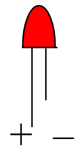
LED stands for light-emitting diode. It is a small electronic component that produces light when electricity flows through it.
-
Longer pin is ''
Resistors
Resistors are electronic components that produce resistance in an electrical circuit, limiting the current/diving the voltage in a circuit. They reduce the flow of electricity and convert extra electrical energy into heat.
The relationship between resistance, current and voltage for linear circuits is modelled by Ohm’s Law.
Internal Resistance
All electrical components produce resistance in a circuit, often known as internal resistance. Most circuit components that consumer power, such as electric motors, are often modelled as resistors to simplify circuit analysis.
The internal resistance of other components, such as voltage/current sources, batteries or even wires, are modelled by adding an ideal ‘internal resistor’ in series with that component.
Resistance Values
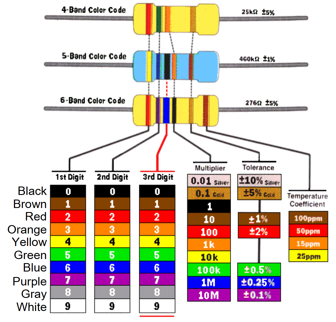
Resistors are too small to print their resistance directly on the component. Thus, we use a colour coded system to indicate the resistance, tolerance and temperature coefficient of resistors.