Types of Memory
ROM Read Only Memory
- Read only
- Keeps data when powered down
RAM Random Access Memory - Read/Write access
- Loses data when powered down
ROM
- Keeps data when powered down
- Contents cannot be changed
- Used for system boot
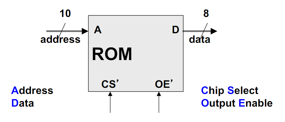
Types of ROM
- ROM Read Only Memory
- Can never be changes
- PROM Programmable ROM
- Comes empty
- Can be ‘programmed’ but changes are permanent
- EPROM Erasable Programmable ROM
- Original state can be restored through UV exposure
- EEPROM Electronically Erasable Programmable ROM
- Can be electrically programmed/erased many times
ROM Implementation
The basic schematic of a ROM implementation consists of three primary components:
- Address Inputs (): specify which byte in memory is selected
- Decoder: an -to-2 decoder takes input address lines and activates exactly one output row line corresponding to that address
- Data Bus / Column Lines (): the output lines that display the byte stored at the activated address line
The horizontal lines are connected to any number of vertical lines through either a diode or transistor connection. When a singular horizontal line is powered by the decoder, it activates the connected vertical output lines.
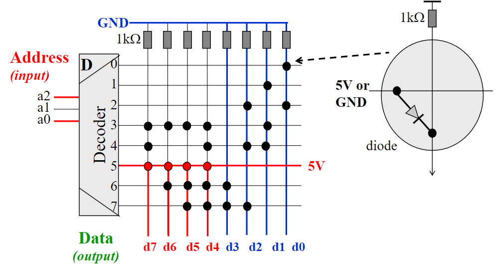
As we can see, the diode/transistor connections are persistent and will remain the same even if the ROM is powered off.
RAM
- Loses data when powered down
- Content can be changed at any time
- Can store programs or data
There are two types of RAM: static RAM and dynamic RAM. SRAM is more expensive and works as intended. DRAM is cheaper, but ‘leaks’ memory contents over short time period -> requires periodic ‘refresh’ every memory cell.
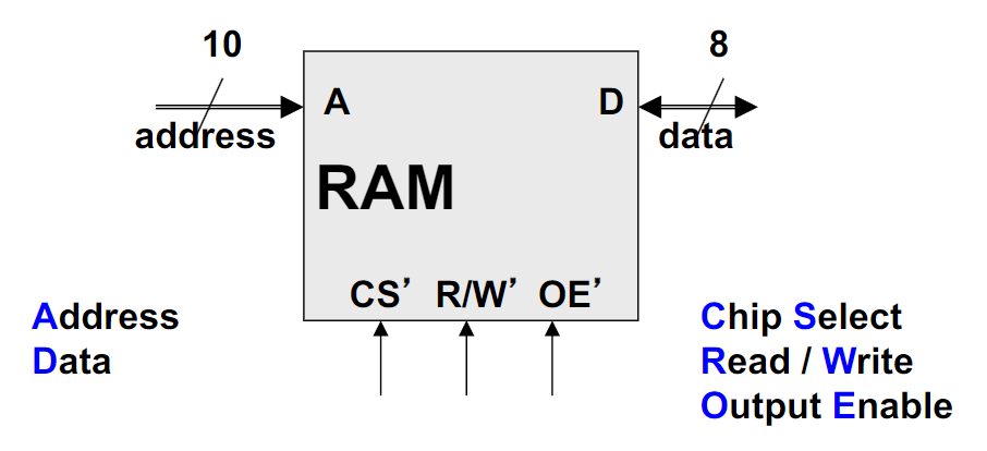
RAM Implementation
RAM implementation is similar to ROM, but we replace the connection element '' by an active switch.
DRAM has only one Field-Effect Transistor (FET) per bit but requires a ‘refresh’ operation every ~64ms for the whole memory.
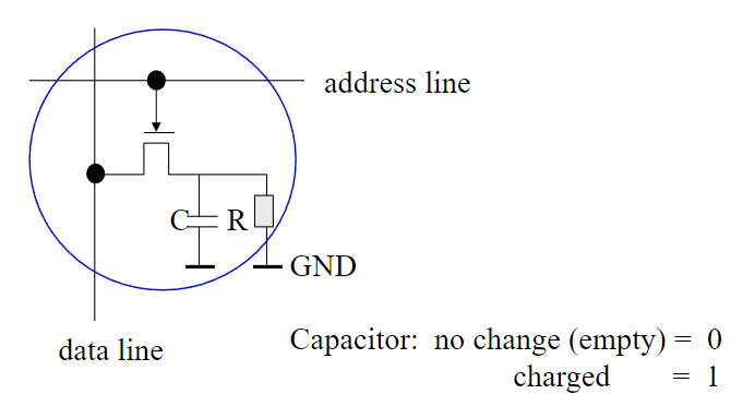
SRAM uses 6 FETs per bit using CMOS (Complimentary Metal Oxide Silicon) technology.
Memory Size
One Byte = Eight Bits
Memory Sizes
- Kilobyte (KB = Bytes = Bytes)
- Megabyte (MB = KB = Bytes)
- Gigabyte (GB = MB = Bytes)
- Terabyte (TB = GB = Bytes
Note: upper-case symbols (KB, MB, etc.) follow traditional computing memory sizes (KB = 1024), but lower-case symbols (kB, mB, etc.) are rounded using decimal math (kB = 1000).
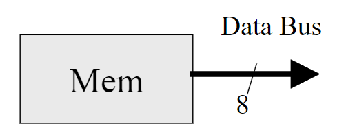
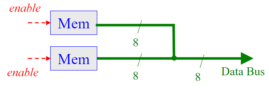
We call a set of 8 data lines a data bus. Instead of running two bytes of memory on two bus lines, we instead reuse the same line. Only one device is allowed to send data at a time. We ensure this through the use of tri-state buffers.
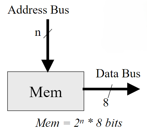
Given our address lines have a bus size of , we can store bytes!
Memory Control
We use several control lines to control our memory chips:
- Chip-SELECT’ -> activate memory chip
- Output-ENABLE’ -> write data to bus
- Read/Write’ -> activate writing (RAM only)
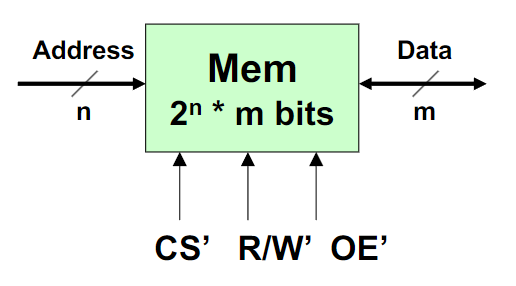
These control lines turn ON when they are unpowered (logical ‘0’) which is indicated by the in their name. This is the standard for most memory chips. You can set a control line to always be ON by routing it to ground.
Address Space
A memory cell’s width is called a word. We can calculate the total size of a memory module through the formula:
Memory module sizes are always in powers of 2. We increase the number of address lines by one starting with one line for 2 cells.
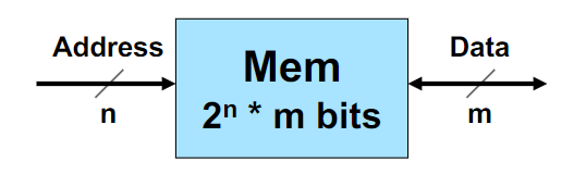
The number of data lines required is equal to the number of bits in the memory cell.