Function Units
Function units have one or two inputs and one output, such as an adder. Our inputs can be words (e.g. 8 bit lines) and our outputs could also be words or just a single bit.
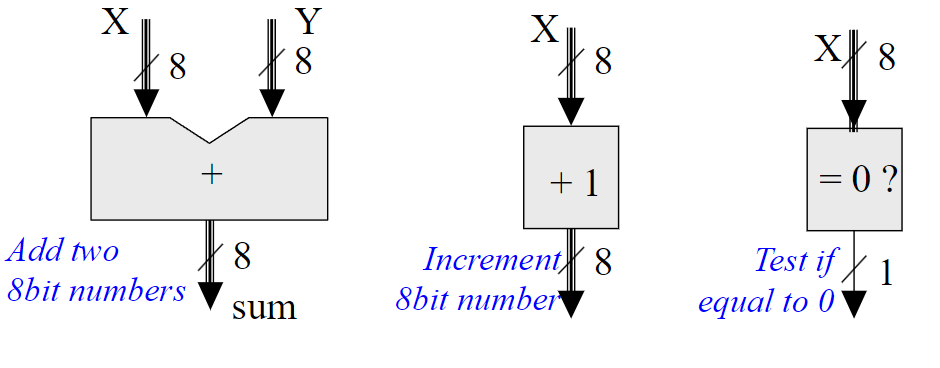
Some examples of basic function units and their implementation:
- Add +1 -> adder or half adders
- Is = 0 ? -> use NOR gates
- Output negative (2’s Complement) -> NOT then +1
- Two inputs equal? -> subtract then is = 0?
There are usually multiple implementations for the same function unit. If there are multiple steps in implementing a unit, look to combine parts/gates to simplify your circuit.
Registers
Registers
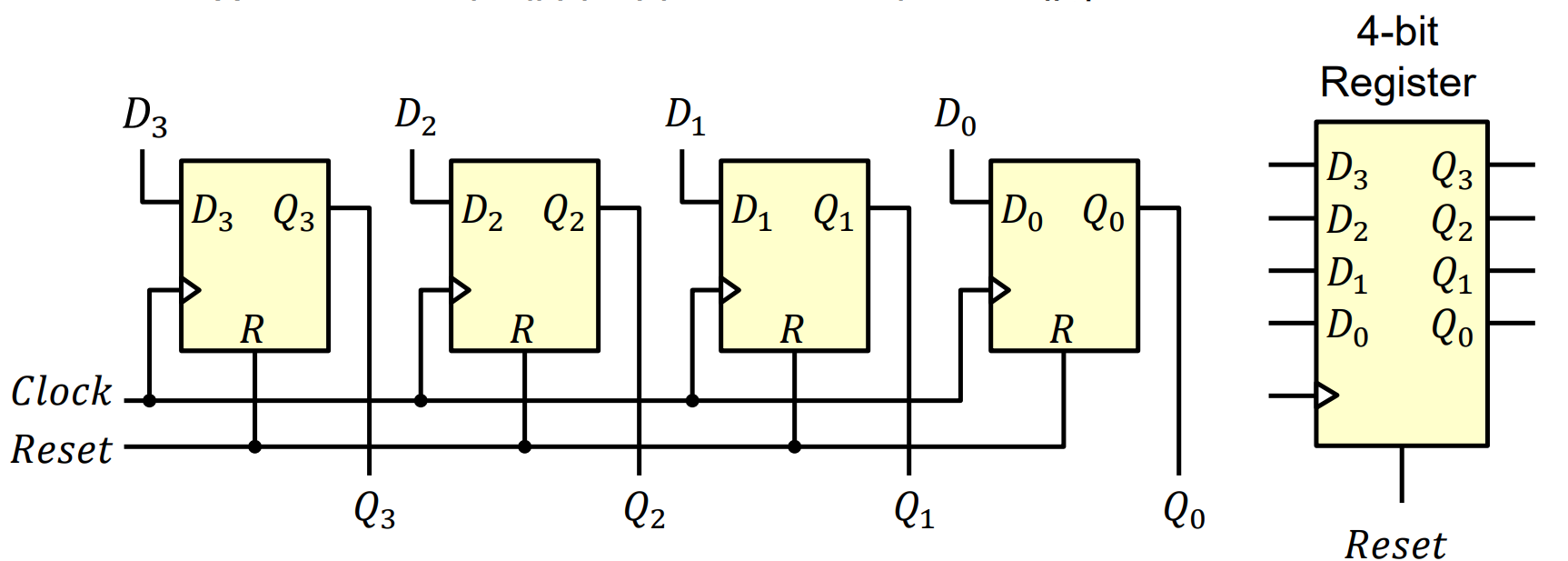
- Registers can hold more data than individual flip-flops
- A -bit register consists of flip-flops and stores bits
Example internal circuitry of a 4-bit register:
Link to original
- All the flip-flops share common Clock and Reset signals
- Common clock: data is loaded in parallel at same clock edge
- Common reset: all Flip-Flops are reset in parallel
Hardware Description Languages
Examples:
- VHDL
- Verilog
- Lola (logic language)
- Retro Graphics Editor -> used in this unit
Central Processing Unit (CPU)
A CPU consists of two main units: an Arithmetic Logic Unit (ALU) and a Control Unit (CU).
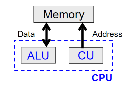
Additionally, a CPU must have a command table and signal timing.
Arithmetic Logic Unit (ALU)
The Arithmetic Logic Unit takes input data from memory and performs operations on the data in its Function Block.
The Function Block is composed of many different function units. A function code selects which operation to perform. An example of a function block implementation would be a multiplexer with different logic gates on each line.
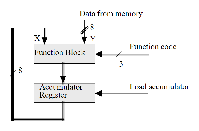
The output of the function block goes to the Accumulator Register to be stored temporarily. This is then fed back into the function block. The load accumulator line comes from the control unit and decides whether the ALU updates the accumulator register or holds onto the old data.
Control Unit (CU)
The Control Unit is responsible for delivering instructions and managing data flow around the CPU. It manages the execution of every program by driving the CPU through the Instruction Cycle (Fetch-Decode-Execute).
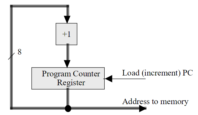
The control unit composes of the Program Counter Register and a +1 incrementer. The register holds the memory address of the current instruction. It can easily increment its stored address by one whenever it receives a signal from the Load PC line.
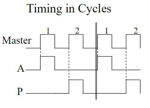
The Accumulator Register and PC Register in a CPU should not activate on the same clock tick. Instead, they should alternate such that an address is loaded, and then the ALU operates on it. This can be implemented through wiring both registers to a pulse generator that pulses two lines at alternating ticks.
Advanced CPU Design
Branching
Typically, a processor increments its Program Counter (PC) sequentially to fetch and execute instructions one after another. A branching instruction breaks this flow by loading a new destination target address directly into the PC register.
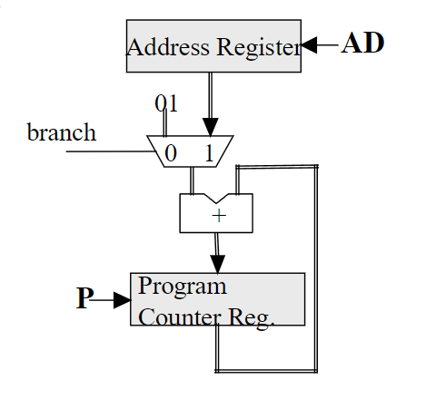
Branching adds more flexibility and efficiency to a CPU, by allowing re-use of code, and dynamically switching execution paths based on inputs.
Types of Branching
There are several types of branching that can depend on decision logic, addressing method or target determination:
- The CPU can jump to a target address with no further conditions or can check for a specific flag or condition register first.
- The instruction can provide an exact memory address to load or an offset value that gets added to the current PC value.
- The target address or offset can be hardcoded or the instruction could point to a register that holds the target address.
Writing to Memory
For more complex functions, we will need to be able to store values in memory during operation. We will use RAM to both load and store data to/from.
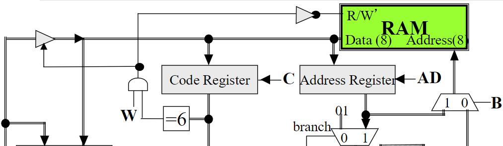
The Read/Write’ function of RAM is controlled by the line:
- -> Read State
- -> Write State
During the write state, the RAM turns its output drivers off and it is safe to connect the Accumulator output to the RAM. The input data is only written into RAM memory on the rising edge () as transitions back to read mode.
In order to prevent a short circuit by accidentally having the RAM and Accumulator output to the Data line concurrently, we must use a tri-state gate.
In the CPU above, WRITE is function 6. When the function code and the clock pulse activates, the tri-state gate connects the Data line to the Accumulator as the RAM switches modes. Then, after the clock pulse, the RAM returns to read mode and stores the data to memory as the tri-state buffer disengages.
In order for this all to work reliably, a set of timing rules must be met: