ELEC1303 - Lecture 4
Logic Gates - Slides
Recap: Logic Gates and Symbols
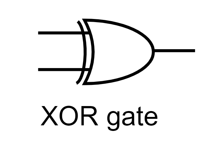
XOR and NXOR Gates
- eXclusive OR (XOR) is an important Boolean operation
- The XOR operation can be written with a circled plus sign between variables:
- There is also an XNOR gate, which is the compliment of XOR
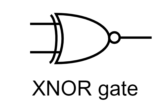
When you have N inputs for a XOR gate (i.e. N > 2), it produces a HIGH (1) when an odd number of inputs are HIGH (1)
Gate Delay
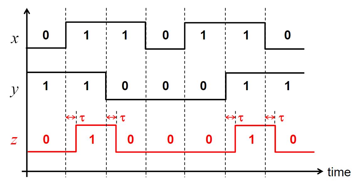
- Output changes do not occur instantaneously
- Delay between an input and output change is the gate delay
- We denote this by
Rise-Time and Fall-Time
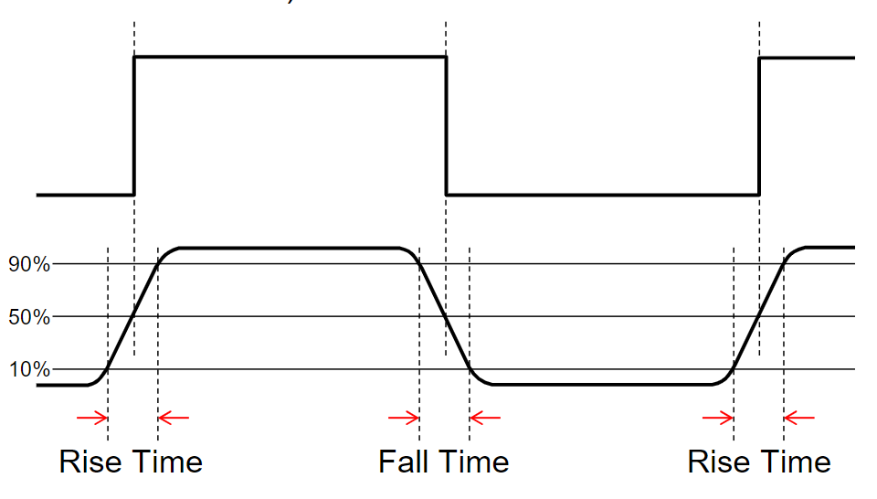
- In logic simulators, we depict switching between logic levels (from 0 to 1 and vice-versa) as instantaneous
- In reality, a signal has a non-zero rise-time and fall-time
- This is the time taken to change from 0 to 1 and vice-versa
Timing Diagrams
- Timing diagrams depict the functional behaviour of a logic circuit in a form that can be observed when the circuit is tested
- See slides for an example
Universal Gates
- Universal gates can implement any Boolean function
- NAND/NOR gates are universal gates because one can implement any logic function using only NOR or only NAND
Universal Gate - NOR
- NOR is a universal gate because one can implement any logic function using only NOR gates
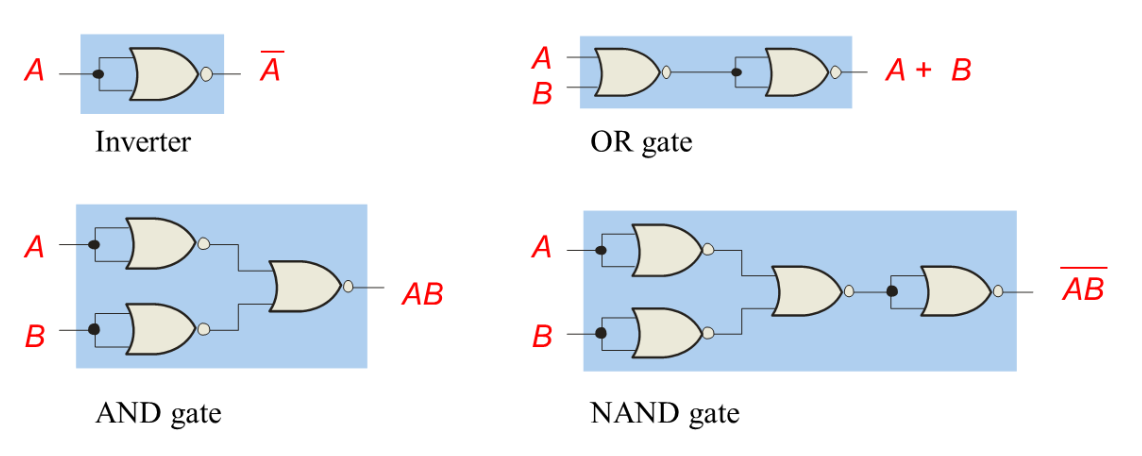
- NOR gate is preferred to OR gate because it can be implemented more efficiently in CMOS technology
Universal Gate - NAND
- NAND is a universal gate because one can implement any logic function using only NAND gates
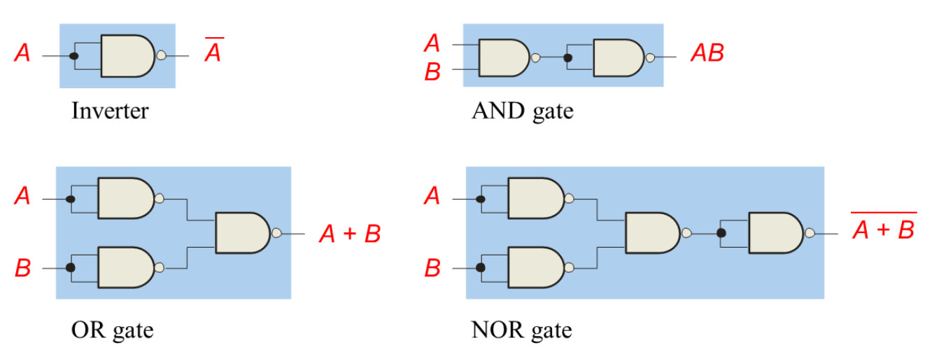
- NAND gate is preferred to AND gate because it can be implemented more efficiently in CMOS technology
Remember that inverters cancel each other out and this can help with trying to find the most efficient circuit using NAND/NOR gates
e.g. two AND gate formations running into an OR gate formation becomes just two NAND gates!
Recall:
Fan-in of a Logic Gate
- The fan-in of a gate is its number of inputs
- Propagation delay increases exponentially with fan-in of gate
- You should avoid logic gates with fan-in greater than 4
Logic Optimisation
- Synthesizing an optimized circuit is a very complex problem
- Boolean simplification
- Mapping to cell libraries with many gates
- Multi-dimensional trade-offs
- e.g. minimize area- delay-power product
- Only possible to do by hand for small circuits
Fan-out of a Logic Gate
- Common for output to be connected to input of several gates
- When this happens, output gate is called driver gate
- The fan-out of a gate is the number of inputs it can feed
- There is a limit of the maximum fan-out of a gate
- This is because a gate can supply only so much current
- Each input gate consumes some amount of current
Buffer Gate
- A buffer is used to improve circuit voltage levels and increase fan-out and speed of circuit
- Buffer gate
- Output = Input
Logic Chips
- In the labs, we will be using integrated circuits
- The pins on these circuits are numbered
- Ordered counter-clockwise
- Each integrated circuit may belong to different families
- Its important for now to just focus on each chips functionality
Some chips we will be using:
7400 NAND four 2-input NAND gates
7404 Inverters six inverters
7402 NOR four 2-input NOR gates